New Undergraduate Research Opportunity at Smart Materials Solutions

Smart Material Solutions, Inc. (SMS) is seeking two REU students for 10 week paid summer internships. SMS is a small NC State startup in Raleigh, NC that is developing an advanced nanomanufacturing process called nanocoining. The patented process can seamlessly nanopattern drum molds for roll-to-roll manufacturing hundreds of times faster than competing technologies like electron-beam lithography.

Internship 1: Simulations of optical properties
This student will perform finite different time domain (FDTD) simulations to model and optimize the optical properties of nanostructures. The intern will model anti-reflective coatings as well as light-extraction features for OLED displays and solid-state lighting. This student will also be trained in scanning electron microscopy (SEM) and atomic force microscopy (AFM). Students with a background in optics, modeling, physics, electrical engineering, or a related field are encouraged to apply.

Internship 2: Fabrication, characterization, and lamination of nanostructured films
This intern will imprint nanostructures into polymer films and characterize their optical and wetting properties. The student will also laminate nanostructures onto devices such as a solar cell and smartphone. This student will receive training on several characterization techniques including SEM, AFM, and UV-Vis spectroscopy. SMS prefers a student with a background in materials science, chemical engineering, nanotechnology, or a related field.

For more information, please review this flier. To apply, send your resume to miller@smartmaterialsolutions.com and specify which internship interests you.

Many new tools online or coming soon!

The RTNN has several new tools that have come online recently, and there are also several instruments scheduled to come into the facilities in the next few months. For technical questions about these tools or reservation information, please contact rtnanonetwork@ncsu.edu.


Online and ready for use:

  • The NNF recently acquired a Heidelberg Instruments µPG 101 direct write lithography system. This system is equipped with a 375 nm ultraviolet diode laser capable of exposing feature sizes down to 0.8 µm on either positive or negative photoresists on sample sizes of 10 x 10 mm up to 5 x 5”. In addition to full exposure, it has the ability to create surface topographies for gray scale applications.
  • The Analytical Instrumentation Facility’s Horiba H-CLUE Spectroscopy & Imaging Catholuminescence (CL) system is now available for users on the JEOL 7600 scanning electron microscope (SEM). CL is a non-destructive spectroscopy technique that provides electronic-structure information via optical emissions induced by the electron-beam excitation. Similar to photoluminescence spectroscopy, but performed in an SEM, CL spectra can be collected at nanometer spatial resolution to probe electronic-structure inhomogeneities in materials. The technique can be used to induce and image surface plasmon resonances in nanostructured materials. The H-Clue offers wide spectral range from UV to IR, 200-2200 nm (6.2 – 0.56 eV). The technique is particularly suitable for analysis of wide-band semiconductors, photonic and polaritonic nanostructures, dielectric oxides and minerals.
  • A new detector named “Symmetry” is now available on the FEI Verios SEM at the AIF, providing superior orientation microscopy capabilities. The image at the right is a representative Electron Backscatter Diffraction (EBSD) map of a deformed Ni alloy specimen collected at ~1500 pixels per second, which is more than an order of magnitude faster than possible with the other detector. Speeds up to 3200 pixels/second are achievable, even at reduced operating voltages and beam currents, allowing data collection on poorly conducting specimens

Coming Soon:

  • An Asylum Research Cypher AFM has just been installed in SMIF. It will be available to users in mid-April 2018.
  • The FEI Krios Cryo-TEM in SMIF will offer atomic scale resolution of samples held at cryogenic temperatures. Its cryo-based technology and stability allow for single particle analysis and dual-axis cellular tomography of frozen hydrated cell organelles and cells. The TEM is equipped with a robotic loader, capable of handling up to 12 frozen hydrated samples for increased throughput.It will be available to users in late April 2018.
  • Installation and start-up of an FEI Apreo SEM at SMIF is expected to begin this month. The new SEM should be available to users in early May 2018.
  • CHANL will be bringing a new Rigaku SmartLab XRD system online in May/June of 2018.  This system will be capable of looking at powders and thin film samples.  In addition to traditional XRD experiments, it is also capable of in-plane diffraction and SAXS, and there are options for working with samples in inert environments and at various temperatures.
  • The NNF has acquired an Annealsys AS-One 150. This rapid thermal processing tool is capable of running samples from small pieces to 6” wafers, up to 1300˚C with pressure ranges from atmospheric conditions to high vacuum. It will become available to users in May 2018.
  • The AIF will install an FEI Talos TEM that will become available to users in late summer 2018. This instrument comes as the result of an MRI award granted to Professor Jim LeBeau.
  • CHANL is adding a Bruker Hyperion FTIR microscope capable of transmission and attenuated total reflectance (ATR) measurements from 600 to 7500 cm-1 with 1 cm-1 spectral resolution. It will map spectra with a lateral resolution ranging from 20 to 250 µm. The system is projected to be online in summer or fall 2018.

New equipment in the RTNN!

The RTNN has several new tools online with many more scheduled for installation in the coming months. Please contact rtnanonetwork@ncsu.edu with any questions regarding technical information or access.

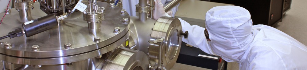
FEI Titan Krios Cryo-Transmission Electron Microscope (Cryo-TEM): This 300 keV instrument offers atomic scale resolution of samples held at cryogenic temperatures and is the most powerful and flexible high-resolution electron microscope for 2D and 3D characterization of biological samples on the market.  Its cryo-based technology and stability allows for single particle analysis and dual-axis cellular tomography of frozen hydrated cell organelles and cells.  The TEM is equipped with a robotic loader, capable of handling up to 12 frozen hydrated samples for increased throughput. Lab renovations are underway for this new Cryo-TEM.

Atomic Force Microscope (AFM): The Asylum AFM includes an MFP-3D head, an XY scanner, and a base. The MFP-3D head offers low noise and precise measurements of the cantilever position for accurate force and topography measurement. The XY-scanner provides flat scans and the ability to accurately zoom and offset with one mouse click. The 3D base offers three configurations for illuminating and viewing samples: top view for opaque samples, bottom view for transparent samples, and dual view for both viewing options.

Raman Microscope: This XploRA PLUS Confocal Raman Microscope includes integrated imaging spectrometer with 4 gratings mounted on motorized turret for full resolution, range and coverage as well as low noise full range CCD detector. It comes with motorized computer controlled 6 position ND filter wheel, confocal pinhole, entrance slit and coupling optics, laser and filter selection. The instrument includes 532 nm and 785 nm Raman excitation laser sources. It offers fast confocal imaging, automated laser wavelength switching. It provides sample identification and chemical imaging on a microscopic scale.

Atomic Layer Deposition (ALD): A newly installed ALD system has allowed us to add 6 precursor lines in one of the facilities, including a low vapor pressure (LVP) delivery line, and has also relieved scheduling pressure that users were experiencing on the original system.  New precursors that we have been exploring since the purchase of the new system include a number of metal organics for depositing CuO, Ga2O3, HfO2, Nb2O5, WO3, and ZnO. The Ultratech Fiji 200Gen 2 Plasma ALD system has four precursor locations and four gas lines into the system for depositions. This instrument is a modular, high-vacuum system that accommodates a wide range of deposition modes.

E-beam lithography: A new Nanometer Pattern Generation System (NPGS) system was installed in one of our focused ion beam (FIB) systems. The NPGS is designed as an e-beam lithography system, but can also be used with the focused ion beam as well.  The system can achieve for patterning with resolution on the order of less than 20 nm for the electron beam and less than 50 nm for the ion beam.

Maskless Lithography System: The Heidelberg Instruments µPG 101 is a direct write lithography system equipped with a 375 nm ultraviolet diode laser capable of exposing feature sizes down to 0.6 µm on either positive or negative photoresists on samples sizes of 10 mm x 10 mm up to 6” x 6”. In addition to full exposure, it has the ability to create surface topographies for gray scale applications.

Reactive ion etcher: The Oxford Plasmalab100 is an induced coupled plasma etcher dedicated to GaN etching.

Cathodoluminescence Imaging and Spectroscopy Detection: The Horiba HCLUE will be installed on our cryo-scanning electron microscope this fall. The spectroscopy system has a focal length of 320 mm and will operate in the ultraviolet-visible range (200-1050 nm). Panchromatic or monochromatic imaging is available in the system.

Retractable Detectors: Two new detectors will be installed on our dual beam FIB/SEM. The retractable annular scanning transmission electron microscope (STEM) detector enables scanning transmission imaging in bright field, dark field, and high-angle dark field modes. The detector includes a special sample holder that can hold up to 6 transmission electron microscopy (TEM) grids and is compatible with the holder used for thin sample preparations. The retractable directional backscatter (DBS) detector features four concentric ring segments that enable separate detection of electrons emitted at different angles. This detector is an ultra-sensitive, Solid State (SS) detector which is sensitive to emitted electrons from 500 V onwards. Using the option beam deceleration, images with beam landing energies down to 50 V are possible. This detector is mounted on a software-controlled retractable arm and allows simultaneous energy dispersive X-ray spectroscopy (EDS) spectra acquisition for WD ≥ 10 mm.

Rapid Thermal Processor: The Annealsys AS-One 150 is a rapid thermal processing tool that will be capable of running samples from small pieces to 6” wafers, up to 1300˚C with pressure ranges from atmospheric conditions to high vacuum.