Scanning Electron Microscopy Short Course

February 8, 2019 @ 9:00 am 5:00 pm

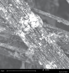
The goal for the day is to learn the basics of scanning electron microscopy (SEM) theory and SEM operation so that you can apply that knowledge to analyzing your own samples and/or understanding what SEM data means. Please note that a short course is designed to teach you how the technique works, the data that can be derived thereof, and what the generated data means. Training is designed to teach you the operational specifics of a particular instrument. Assuming that all is well you should be able to drive the Hitachi S-3200N SEM more or less independently by the end of the day. That said, it is not unusual for users to request additional training for a particular instrument.

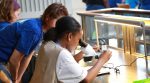
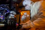
We will start with an introduction lecture to SEM after which we will move to the lab. In the first lab, the student will observe a demonstration of SEM operation.  Then each of you will drive the microscope on a standard sample and we will explore changing instrument conditions and the resulting effect on the data. During this phase, we will also learn how to focus and correct astigmatism as well as how to properly set signal gain (contrast) and offset (brightness). After a break for lunch, there will be another lecture where we learn more about electron beam-sample interactions, detectors, how to pick imaging conditions, etc. Then we will go to the lab where you can apply what you have learned by imaging any sample you wish. You are welcome to bring a sample for this time or I can find one that is appropriate.

You should bring something to write with and on, a memory stick for the presentation and any data or other information that is electronic, and last but certainly not least, your brain. You can also bring a sample for hands-on time in the afternoon. We will take a short break for lunch, probably on the order of 30-45 minutes, so it might be smart to bring lunch with you.

This should be a relaxed and enjoyable day where you learn something fun and useful. Questions? Please contact Chuck Mooney at cbmooney@ncsu.edu. To maximize hands-on time, the class is limited to three students.

Registration costs: $50 for academic, government, and non-profit participants; $350 for industry participants

To register, add yourself to the short course through AIF’s lab management software, Mendix. Click here to watch a short video on how to register for a short course in Mendix. Select “Sign up for a Short Course.”

2410 Campus Shore Drive
Raleigh, NC United States
+ Google Map

Girls STEM Day @ Duke Fuels the STEM Pipeline

On Saturday, May 19th, Girl Scouts and their families traveled to Duke University to learn from and work with over 100 women in STEM careers across the Triangle. Girl Scouts earned badges in digital photography, forensics, and robotics through a variety of different activities including use of SMIF’s scanning electron microscope. In a parallel parents forum, female STEM professionals, high school college counselors and university admissions counselors engaged parents and troop leaders in interactive panel discussions. To learn more about the event and see more photos, read Duke’s News Release.

Participants earning the digital photography badge were charged with imaging samples that they collected with both light and electron microscopes. These ranged from a flower petal (below image top) to a bagel (below image bottom).


New Undergraduate Research Opportunity at Smart Materials Solutions

Smart Material Solutions, Inc. (SMS) is seeking two REU students for 10 week paid summer internships. SMS is a small NC State startup in Raleigh, NC that is developing an advanced nanomanufacturing process called nanocoining. The patented process can seamlessly nanopattern drum molds for roll-to-roll manufacturing hundreds of times faster than competing technologies like electron-beam lithography.

Internship 1: Simulations of optical properties
This student will perform finite different time domain (FDTD) simulations to model and optimize the optical properties of nanostructures. The intern will model anti-reflective coatings as well as light-extraction features for OLED displays and solid-state lighting. This student will also be trained in scanning electron microscopy (SEM) and atomic force microscopy (AFM). Students with a background in optics, modeling, physics, electrical engineering, or a related field are encouraged to apply.

Internship 2: Fabrication, characterization, and lamination of nanostructured films
This intern will imprint nanostructures into polymer films and characterize their optical and wetting properties. The student will also laminate nanostructures onto devices such as a solar cell and smartphone. This student will receive training on several characterization techniques including SEM, AFM, and UV-Vis spectroscopy. SMS prefers a student with a background in materials science, chemical engineering, nanotechnology, or a related field.

For more information, please review this flier. To apply, send your resume to miller@smartmaterialsolutions.com and specify which internship interests you.

Many new tools online or coming soon!

The RTNN has several new tools that have come online recently, and there are also several instruments scheduled to come into the facilities in the next few months. For technical questions about these tools or reservation information, please contact rtnanonetwork@ncsu.edu.


Online and ready for use:

  • The NNF recently acquired a Heidelberg Instruments µPG 101 direct write lithography system. This system is equipped with a 375 nm ultraviolet diode laser capable of exposing feature sizes down to 0.8 µm on either positive or negative photoresists on sample sizes of 10 x 10 mm up to 5 x 5”. In addition to full exposure, it has the ability to create surface topographies for gray scale applications.
  • The Analytical Instrumentation Facility’s Horiba H-CLUE Spectroscopy & Imaging Catholuminescence (CL) system is now available for users on the JEOL 7600 scanning electron microscope (SEM). CL is a non-destructive spectroscopy technique that provides electronic-structure information via optical emissions induced by the electron-beam excitation. Similar to photoluminescence spectroscopy, but performed in an SEM, CL spectra can be collected at nanometer spatial resolution to probe electronic-structure inhomogeneities in materials. The technique can be used to induce and image surface plasmon resonances in nanostructured materials. The H-Clue offers wide spectral range from UV to IR, 200-2200 nm (6.2 – 0.56 eV). The technique is particularly suitable for analysis of wide-band semiconductors, photonic and polaritonic nanostructures, dielectric oxides and minerals.
  • A new detector named “Symmetry” is now available on the FEI Verios SEM at the AIF, providing superior orientation microscopy capabilities. The image at the right is a representative Electron Backscatter Diffraction (EBSD) map of a deformed Ni alloy specimen collected at ~1500 pixels per second, which is more than an order of magnitude faster than possible with the other detector. Speeds up to 3200 pixels/second are achievable, even at reduced operating voltages and beam currents, allowing data collection on poorly conducting specimens

Coming Soon:

  • An Asylum Research Cypher AFM has just been installed in SMIF. It will be available to users in mid-April 2018.
  • The FEI Krios Cryo-TEM in SMIF will offer atomic scale resolution of samples held at cryogenic temperatures. Its cryo-based technology and stability allow for single particle analysis and dual-axis cellular tomography of frozen hydrated cell organelles and cells. The TEM is equipped with a robotic loader, capable of handling up to 12 frozen hydrated samples for increased throughput.It will be available to users in late April 2018.
  • Installation and start-up of an FEI Apreo SEM at SMIF is expected to begin this month. The new SEM should be available to users in early May 2018.
  • CHANL will be bringing a new Rigaku SmartLab XRD system online in May/June of 2018.  This system will be capable of looking at powders and thin film samples.  In addition to traditional XRD experiments, it is also capable of in-plane diffraction and SAXS, and there are options for working with samples in inert environments and at various temperatures.
  • The NNF has acquired an Annealsys AS-One 150. This rapid thermal processing tool is capable of running samples from small pieces to 6” wafers, up to 1300˚C with pressure ranges from atmospheric conditions to high vacuum. It will become available to users in May 2018.
  • The AIF will install an FEI Talos TEM that will become available to users in late summer 2018. This instrument comes as the result of an MRI award granted to Professor Jim LeBeau.
  • CHANL is adding a Bruker Hyperion FTIR microscope capable of transmission and attenuated total reflectance (ATR) measurements from 600 to 7500 cm-1 with 1 cm-1 spectral resolution. It will map spectra with a lateral resolution ranging from 20 to 250 µm. The system is projected to be online in summer or fall 2018.

RTNN acquires portable Scanning Electron Microscope

Through collaboration with the Parsons Research Group at NC State, the RTNN now has available a PhenomWorld Desktop SEM. The Phenom SEM allows for very fast microscopic imaging of samples in a compact, portable package – about the size of a desktop computer. The RTNN will use the Desktop SEM in outreach programs, such as bringing instruments to classrooms for demonstrations of instruments used in nanoscience. If you are interested in having the RTNN bring the desktop SEM to your event or school, please contact Phillip Strader (phillip_strader@ncsu.edu) or Maude Cuchiara (maude_cuchiara@ncsu.edu)